
راه اندازی ماژول دوربین OV7670 :
OV7670 یک سنسور CMOS با ابعاد 1/6 اینچ و همچنین 0.3 مگاپیکسل است . این سنسور در شکل های مختلفی در بازار وجود دارد که در همه آن ها چیپ OV7670 به کار رفته است . در این آموزش ما از مدل دارای پین هدر استفاده می کنیم چراکه به کار گیری آن برای اتصال به برد هایی همچون آردوینو ، راحت تر است .
یکی از مهمترین مزیت های OV7670 قیمت پایین آن نسبت به بقیه ماژول های دوبین است ، اما خب راه اندازی آن نیز کمی مشکل خواهد بود . OV7670 از فرمت های زیادی در تصویر برداری پشتیبانی می کند . در بازار چیپ ها و ماژول های دوربین مختلفی وجود دارند که می توانید آن ها را به انواع میکرو کنترلر های و برد ها متصل کنید . اما نکته ای که راجب به این دوربین ها وجود دارد قیمت بالای آن ها می باشد . ما در این آموزش راه اندازی OV7670 بدون FIFO را خواهیم گفت . شاید در عمل به دلیل سرعت پایین آردوینو در دریافت خروجی دوربین ، نرخ فریم های دریافتی بسیار پایین باشد اما نکته مهم در این آموزش راه اندازی OV7670 در پلتفرم های دیگر است .
مشخصات ماژول OV7670 :
- اندازه دریچه 1/6 اینچ
- وضوح تصویر 640×480
- ولتاژ تغذیه 3.3 ولت
- حساسیت بالا در نور کم
- توابع خودکار برای تنظیماتی همچون AGC ،AEC ، AWB و…
- فیلتر سطح سیاه (ABF و ABLC )
- تنظیم لبه تصویر
- فیلتر نویز های 50Hz تا 60Hz
- رابط ارتباطی I2C برا کنترل و رابط پارلل برای خروجی تصویر
شاید در نگاه اول کیفیت 640×480 این دوربین پایین به نظر بیاد . اما باید به این نکته توجه داشت که این دوبین برای گرفتن عکس یادگاری طراحی نشده است بلکه برای استفاده در سیستم های امبدد در جهت پردازش تصویر ساخته شده . می توان از این ماژول در سیستم های سورتینگ و… استفاده کرد .
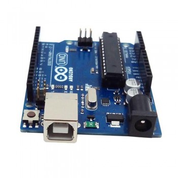
در این آموزش به وسایل زیر نیاز دارید :
راه اندازی OV7670 :
قبل از اجرای برنامه بهتر است به الگوی راه اندازی این ماژول بپردازیم . OV7670 علاوه بر سیگنال تغذیه 3.3 ولتی ، به پالس ساعت 10 تا 48MHz نیز احتیاج دارد که این پالس با دیوتی سایکل 50 درصدی باید به پین XCLK اعمال شود . این دوربین دارای رابط ارتباطی I2C جهت تنظیم رجیستری ها است . در این مثال از مقادیر پیش فرض رجیستری ها استفاده می شود و تنها رجیستر های مربوط به ابعاد تغییر داده می شوند . پس از پیکر بندی دوربین (تغییر رجیستری ها به مقدار مد نظر از طریق رابط I2C ) دوربین شروع به کار خواهد کرد و مقادیر هر پیکسل را به ترتیب از پیکسل اول تا اخرین پیکس به خروجی می فرستد . خروجی این ماژول شامل 8 پین است که مقدار هر پیکسل به صورت 8 بیتی بر روی این هشت پین قرار می گیرد . همچنین از دو پایه VSYNC و HREF برای سیگنال های همگام سازی استفاده می شود (با ارسال مقدار هر پیکسل این پین ها تغییر وضعیت می دهند ) .
در این مثال مقادیر خوانده شده برای هر پیکس از تریق پورت سریال به کامپیوتر ارسال می شود و در آن جا با استفاده از نرم افزار قرار داده شده در این لینک تصاویر را مشاهده و با ذخیره نمود .
از شماتیک زیر برای اتصال OV7670 به آردوینو استفاده کنید :
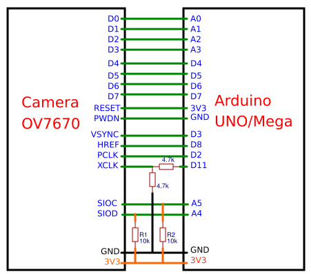
پس از اتصال OV7670 به آردوینو مطابق شماتیک فوق ، باید کد های زیر را در آردوینو IDE کپی و سپس بر روی آردوینو آپلود کنید . در این شماتیک ممکن است اسامی برخی از پین ها با اسامی نوشته شده بر روی ماژول شما اندکی فرق داشته باشند .
کد های آردوینو :
#include <stdint.h>
#include <avr/io.h>
#include <util/twi.h>
#include <util/delay.h>
#include <avr/pgmspace.h>

#define F_CPU 16000000UL
#define vga   0
#define qvga  1
#define qqvga   2
#define yuv422  0
#define rgb565  1
#define bayerRGB  2
#define camAddr_WR  0x42
#define camAddr_RD  0x43

/* Registers */
#define REG_GAIN    0x00  /* Gain lower 8 bits (rest in vref) */
#define REG_BLUE    0x01  /* blue gain */
#define REG_RED       0x02  /* red gain */
#define REG_VREF    0x03  /* Pieces of GAIN, VSTART, VSTOP */
#define REG_COM1    0x04  /* Control 1 */
#define COM1_CCIR656  0x40    /* CCIR656 enable */

#define REG_BAVE    0x05  /* U/B Average level */
#define REG_GbAVE   0x06  /* Y/Gb Average level */
#define REG_AECHH   0x07  /* AEC MS 5 bits */
#define REG_RAVE    0x08  /* V/R Average level */
#define REG_COM2    0x09  /* Control 2 */
#define COM2_SSLEEP         0x10  /* Soft sleep mode */
#define REG_PID           0x0a  /* Product ID MSB */
#define REG_VER           0x0b  /* Product ID LSB */
#define REG_COM3    0x0c  /* Control 3 */
#define COM3_SWAP         0x40  /* Byte swap */
#define COM3_SCALEEN          0x08  /* Enable scaling */
#define COM3_DCWEN          0x04  /* Enable downsamp/crop/window */
#define REG_COM4    0x0d  /* Control 4 */
#define REG_COM5    0x0e  /* All "reserved" */
#define REG_COM6    0x0f  /* Control 6 */
#define REG_AECH    0x10  /* More bits of AEC value */
#define REG_CLKRC   0x11  /* Clocl control */
#define CLK_EXT           0x40  /* Use external clock directly */
#define CLK_SCALE   0x3f  /* Mask for internal clock scale */
#define REG_COM7    0x12  /* Control 7 */ //REG mean address.
#define COM7_RESET          0x80  /* Register reset */
#define COM7_FMT_MASK         0x38
#define COM7_FMT_VGA          0x00
#define COM7_FMT_CIF          0x20  /* CIF format */
#define COM7_FMT_QVGA         0x10  /* QVGA format */
#define COM7_FMT_QCIF         0x08  /* QCIF format */
#define COM7_RGB          0x04  /* bits 0 and 2 - RGB format */
#define COM7_YUV          0x00  /* YUV */
#define COM7_BAYER          0x01  /* Bayer format */
#define COM7_PBAYER         0x05  /* "Processed bayer" */
#define REG_COM8    0x13  /* Control 8 */
#define COM8_FASTAEC          0x80  /* Enable fast AGC/AEC */
#define COM8_AECSTEP          0x40  /* Unlimited AEC step size */
#define COM8_BFILT    0x20  /* Band filter enable */
#define COM8_AGC    0x04  /* Auto gain enable */
#define COM8_AWB    0x02  /* White balance enable */
#define COM8_AEC    0x01  /* Auto exposure enable */
#define REG_COM9    0x14  /* Control 9- gain ceiling */
#define REG_COM10   0x15  /* Control 10 */
#define COM10_HSYNC         0x40  /* HSYNC instead of HREF */
#define COM10_PCLK_HB         0x20  /* Suppress PCLK on horiz blank */
#define COM10_HREF_REV          0x08  /* Reverse HREF */
#define COM10_VS_LEAD         0x04  /* VSYNC on clock leading edge */
#define COM10_VS_NEG          0x02  /* VSYNC negative */
#define COM10_HS_NEG          0x01  /* HSYNC negative */
#define REG_HSTART    0x17  /* Horiz start high bits */
#define REG_HSTOP   0x18  /* Horiz stop high bits */
#define REG_VSTART    0x19  /* Vert start high bits */
#define REG_VSTOP   0x1a  /* Vert stop high bits */
#define REG_PSHFT   0x1b  /* Pixel delay after HREF */
#define REG_MIDH    0x1c  /* Manuf. ID high */
#define REG_MIDL    0x1d  /* Manuf. ID low */
#define REG_MVFP    0x1e  /* Mirror / vflip */
#define MVFP_MIRROR         0x20  /* Mirror image */
#define MVFP_FLIP   0x10  /* Vertical flip */

#define REG_AEW           0x24  /* AGC upper limit */
#define REG_AEB           0x25    /* AGC lower limit */
#define REG_VPT           0x26  /* AGC/AEC fast mode op region */
#define REG_HSYST   0x30  /* HSYNC rising edge delay */
#define REG_HSYEN   0x31  /* HSYNC falling edge delay */
#define REG_HREF    0x32  /* HREF pieces */
#define REG_TSLB    0x3a  /* lots of stuff */
#define TSLB_YLAST    0x04  /* UYVY or VYUY - see com13 */
#define REG_COM11   0x3b  /* Control 11 */
#define COM11_NIGHT         0x80  /* NIght mode enable */
#define COM11_NMFR          0x60  /* Two bit NM frame rate */
#define COM11_HZAUTO          0x10  /* Auto detect 50/60 Hz */
#define COM11_50HZ          0x08  /* Manual 50Hz select */
#define COM11_EXP   0x02
#define REG_COM12   0x3c  /* Control 12 */
#define COM12_HREF          0x80  /* HREF always */
#define REG_COM13   0x3d  /* Control 13 */
#define COM13_GAMMA         0x80  /* Gamma enable */
#define COM13_UVSAT         0x40  /* UV saturation auto adjustment */
#define COM13_UVSWAP          0x01  /* V before U - w/TSLB */
#define REG_COM14   0x3e  /* Control 14 */
#define COM14_DCWEN         0x10  /* DCW/PCLK-scale enable */
#define REG_EDGE    0x3f  /* Edge enhancement factor */
#define REG_COM15   0x40  /* Control 15 */
#define COM15_R10F0         0x00  /* Data range 10 to F0 */
#define COM15_R01FE         0x80  /*      01 to FE */
#define COM15_R00FF         0xc0  /*      00 to FF */
#define COM15_RGB565          0x10  /* RGB565 output */
#define COM15_RGB555          0x30  /* RGB555 output */
#define REG_COM16   0x41  /* Control 16 */
#define COM16_AWBGAIN         0x08  /* AWB gain enable */
#define REG_COM17   0x42  /* Control 17 */
#define COM17_AECWIN          0xc0  /* AEC window - must match COM4 */
#define COM17_CBAR          0x08  /* DSP Color bar */
/*
* This matrix defines how the colors are generated, must be
* tweaked to adjust hue and saturation.
*
* Order: v-red, v-green, v-blue, u-red, u-green, u-blue
* They are nine-bit signed quantities, with the sign bit
* stored in0x58.Sign for v-red is bit 0, and up from there.
*/
#define REG_CMATRIX_BASE  0x4f
#define CMATRIX_LEN           6
#define REG_CMATRIX_SIGN  0x58
#define REG_BRIGHT    0x55  /* Brightness */
#define REG_CONTRAS         0x56  /* Contrast control */
#define REG_GFIX    0x69  /* Fix gain control */
#define REG_REG76   0x76  /* OV's name */
#define R76_BLKPCOR         0x80  /* Black pixel correction enable */
#define R76_WHTPCOR         0x40  /* White pixel correction enable */
#define REG_RGB444          0x8c  /* RGB 444 control */
#define R444_ENABLE         0x02  /* Turn on RGB444, overrides 5x5 */
#define R444_RGBX   0x01  /* Empty nibble at end */
#define REG_HAECC1    0x9f  /* Hist AEC/AGC control 1 */
#define REG_HAECC2    0xa0  /* Hist AEC/AGC control 2 */
#define REG_BD50MAX         0xa5  /* 50hz banding step limit */
#define REG_HAECC3    0xa6  /* Hist AEC/AGC control 3 */
#define REG_HAECC4    0xa7  /* Hist AEC/AGC control 4 */
#define REG_HAECC5    0xa8  /* Hist AEC/AGC control 5 */
#define REG_HAECC6    0xa9  /* Hist AEC/AGC control 6 */
#define REG_HAECC7    0xaa  /* Hist AEC/AGC control 7 */
#define REG_BD60MAX         0xab  /* 60hz banding step limit */
#define REG_GAIN    0x00  /* Gain lower 8 bits (rest in vref) */
#define REG_BLUE    0x01  /* blue gain */
#define REG_RED           0x02  /* red gain */
#define REG_VREF    0x03  /* Pieces of GAIN, VSTART, VSTOP */
#define REG_COM1    0x04  /* Control 1 */
#define COM1_CCIR656          0x40  /* CCIR656 enable */
#define REG_BAVE    0x05  /* U/B Average level */
#define REG_GbAVE   0x06  /* Y/Gb Average level */
#define REG_AECHH   0x07  /* AEC MS 5 bits */
#define REG_RAVE    0x08  /* V/R Average level */
#define REG_COM2    0x09  /* Control 2 */
#define COM2_SSLEEP         0x10  /* Soft sleep mode */
#define REG_PID           0x0a  /* Product ID MSB */
#define REG_VER           0x0b  /* Product ID LSB */
#define REG_COM3    0x0c  /* Control 3 */
#define COM3_SWAP         0x40  /* Byte swap */
#define COM3_SCALEEN          0x08  /* Enable scaling */
#define COM3_DCWEN          0x04  /* Enable downsamp/crop/window */
#define REG_COM4    0x0d  /* Control 4 */
#define REG_COM5    0x0e  /* All "reserved" */
#define REG_COM6    0x0f  /* Control 6 */
#define REG_AECH    0x10  /* More bits of AEC value */
#define REG_CLKRC   0x11  /* Clocl control */
#define CLK_EXT           0x40  /* Use external clock directly */
#define CLK_SCALE   0x3f  /* Mask for internal clock scale */
#define REG_COM7    0x12  /* Control 7 */
#define COM7_RESET          0x80  /* Register reset */
#define COM7_FMT_MASK         0x38
#define COM7_FMT_VGA          0x00
#define COM7_FMT_CIF          0x20  /* CIF format */
#define COM7_FMT_QVGA         0x10  /* QVGA format */
#define COM7_FMT_QCIF         0x08  /* QCIF format */
#define COM7_RGB    0x04  /* bits 0 and 2 - RGB format */
#define COM7_YUV    0x00  /* YUV */
#define COM7_BAYER          0x01  /* Bayer format */
#define COM7_PBAYER         0x05  /* "Processed bayer" */
#define REG_COM8    0x13  /* Control 8 */
#define COM8_FASTAEC          0x80  /* Enable fast AGC/AEC */
#define COM8_AECSTEP          0x40  /* Unlimited AEC step size */
#define COM8_BFILT    0x20  /* Band filter enable */
#define COM8_AGC    0x04  /* Auto gain enable */
#define COM8_AWB    0x02  /* White balance enable */
#define COM8_AEC    0x01  /* Auto exposure enable */
#define REG_COM9    0x14  /* Control 9- gain ceiling */
#define REG_COM10   0x15  /* Control 10 */
#define COM10_HSYNC         0x40  /* HSYNC instead of HREF */
#define COM10_PCLK_HB         0x20  /* Suppress PCLK on horiz blank */
#define COM10_HREF_REV          0x08  /* Reverse HREF */
#define COM10_VS_LEAD           0x04  /* VSYNC on clock leading edge */
#define COM10_VS_NEG          0x02  /* VSYNC negative */
#define COM10_HS_NEG          0x01  /* HSYNC negative */
#define REG_HSTART    0x17  /* Horiz start high bits */
#define REG_HSTOP   0x18  /* Horiz stop high bits */
#define REG_VSTART    0x19  /* Vert start high bits */
#define REG_VSTOP   0x1a  /* Vert stop high bits */
#define REG_PSHFT   0x1b  /* Pixel delay after HREF */
#define REG_MIDH    0x1c  /* Manuf. ID high */
#define REG_MIDL    0x1d  /* Manuf. ID low */
#define REG_MVFP    0x1e  /* Mirror / vflip */
#define MVFP_MIRROR         0x20  /* Mirror image */
#define MVFP_FLIP   0x10  /* Vertical flip */
#define REG_AEW           0x24  /* AGC upper limit */
#define REG_AEB           0x25  /* AGC lower limit */
#define REG_VPT           0x26  /* AGC/AEC fast mode op region */
#define REG_HSYST   0x30  /* HSYNC rising edge delay */
#define REG_HSYEN   0x31  /* HSYNC falling edge delay */
#define REG_HREF    0x32  /* HREF pieces */
#define REG_TSLB    0x3a  /* lots of stuff */
#define TSLB_YLAST    0x04  /* UYVY or VYUY - see com13 */
#define REG_COM11   0x3b  /* Control 11 */
#define COM11_NIGHT         0x80  /* NIght mode enable */
#define COM11_NMFR          0x60  /* Two bit NM frame rate */
#define COM11_HZAUTO          0x10  /* Auto detect 50/60 Hz */
#define COM11_50HZ          0x08  /* Manual 50Hz select */
#define COM11_EXP   0x02
#define REG_COM12   0x3c  /* Control 12 */
#define COM12_HREF          0x80  /* HREF always */
#define REG_COM13   0x3d  /* Control 13 */
#define COM13_GAMMA         0x80  /* Gamma enable */
#define COM13_UVSAT         0x40  /* UV saturation auto adjustment */
#define COM13_UVSWAP          0x01  /* V before U - w/TSLB */
#define REG_COM14   0x3e  /* Control 14 */
#define COM14_DCWEN         0x10  /* DCW/PCLK-scale enable */
#define REG_EDGE    0x3f  /* Edge enhancement factor */
#define REG_COM15   0x40  /* Control 15 */
#define COM15_R10F0         0x00  /* Data range 10 to F0 */
#define COM15_R01FE         0x80  /*      01 to FE */
#define COM15_R00FF         0xc0  /*      00 to FF */
#define COM15_RGB565          0x10  /* RGB565 output */
#define COM15_RGB555          0x30  /* RGB555 output */
#define REG_COM16   0x41  /* Control 16 */
#define COM16_AWBGAIN         0x08  /* AWB gain enable */
#define REG_COM17   0x42  /* Control 17 */
#define COM17_AECWIN          0xc0  /* AEC window - must match COM4 */
#define COM17_CBAR          0x08  /* DSP Color bar */

#define CMATRIX_LEN             6
#define REG_BRIGHT    0x55  /* Brightness */
#define REG_REG76   0x76  /* OV's name */
#define R76_BLKPCOR         0x80  /* Black pixel correction enable */
#define R76_WHTPCOR         0x40  /* White pixel correction enable */
#define REG_RGB444          0x8c  /* RGB 444 control */
#define R444_ENABLE         0x02  /* Turn on RGB444, overrides 5x5 */
#define R444_RGBX   0x01  /* Empty nibble at end */
#define REG_HAECC1    0x9f  /* Hist AEC/AGC control 1 */
#define REG_HAECC2    0xa0  /* Hist AEC/AGC control 2 */
#define REG_BD50MAX         0xa5  /* 50hz banding step limit */
#define REG_HAECC3    0xa6  /* Hist AEC/AGC control 3 */
#define REG_HAECC4    0xa7  /* Hist AEC/AGC control 4 */
#define REG_HAECC5    0xa8  /* Hist AEC/AGC control 5 */
#define REG_HAECC6    0xa9  /* Hist AEC/AGC control 6 */
#define REG_HAECC7    0xaa  /* Hist AEC/AGC control 7 */
#define REG_BD60MAX         0xab  /* 60hz banding step limit */
#define MTX1            0x4f  /* Matrix Coefficient 1 */
#define MTX2            0x50  /* Matrix Coefficient 2 */
#define MTX3            0x51  /* Matrix Coefficient 3 */
#define MTX4            0x52  /* Matrix Coefficient 4 */
#define MTX5            0x53  /* Matrix Coefficient 5 */
#define MTX6            0x54  /* Matrix Coefficient 6 */
#define REG_CONTRAS         0x56  /* Contrast control */
#define MTXS            0x58  /* Matrix Coefficient Sign */
#define AWBC7           0x59  /* AWB Control 7 */
#define AWBC8           0x5a  /* AWB Control 8 */
#define AWBC9           0x5b  /* AWB Control 9 */
#define AWBC10            0x5c  /* AWB Control 10 */
#define AWBC11            0x5d  /* AWB Control 11 */
#define AWBC12            0x5e  /* AWB Control 12 */
#define REG_GFI           0x69  /* Fix gain control */
#define GGAIN           0x6a  /* G Channel AWB Gain */
#define DBLV            0x6b
#define AWBCTR3           0x6c  /* AWB Control 3 */
#define AWBCTR2           0x6d  /* AWB Control 2 */
#define AWBCTR1           0x6e  /* AWB Control 1 */
#define AWBCTR0           0x6f  /* AWB Control 0 */

struct regval_list{
  uint8_t reg_num;
  uint16_t value;
};

const struct regval_list qvga_ov7670[] PROGMEM = {
  { REG_COM14, 0x19 },
  { 0x72, 0x11 },
  { 0x73, 0xf1 },

  { REG_HSTART, 0x16 },
  { REG_HSTOP, 0x04 },
  { REG_HREF, 0xa4 },
  { REG_VSTART, 0x02 },
  { REG_VSTOP, 0x7a },
  { REG_VREF, 0x0a },

  { 0xff, 0xff }, /* END MARKER */
};

const struct regval_list yuv422_ov7670[] PROGMEM = {
  { REG_COM7, 0x0 },  /* Selects YUV mode */
  { REG_RGB444, 0 },  /* No RGB444 please */
  { REG_COM1, 0 },
  { REG_COM15, COM15_R00FF },
  { REG_COM9, 0x6A }, /* 128x gain ceiling; 0x8 is reserved bit */
  { 0x4f, 0x80 },   /* "matrix coefficient 1" */
  { 0x50, 0x80 },   /* "matrix coefficient 2" */
  { 0x51, 0 },    /* vb */
  { 0x52, 0x22 },   /* "matrix coefficient 4" */
  { 0x53, 0x5e },   /* "matrix coefficient 5" */
  { 0x54, 0x80 },   /* "matrix coefficient 6" */
  { REG_COM13, COM13_UVSAT },
  { 0xff, 0xff },   /* END MARKER */
};

const struct regval_list ov7670_default_regs[] PROGMEM = {//from the linux driver
  { REG_COM7, COM7_RESET },
  { REG_TSLB, 0x04 }, /* OV */
  { REG_COM7, 0 },  /* VGA */
  /*
  * Set the hardware window.  These values from OV don't entirely
  * make sense - hstop is less than hstart.  But they work...
  */
  { REG_HSTART, 0x13 }, { REG_HSTOP, 0x01 },
  { REG_HREF, 0xb6 }, { REG_VSTART, 0x02 },
  { REG_VSTOP, 0x7a }, { REG_VREF, 0x0a },

  { REG_COM3, 0 }, { REG_COM14, 0 },
  /* Mystery scaling numbers */
  { 0x70, 0x3a }, { 0x71, 0x35 },
  { 0x72, 0x11 }, { 0x73, 0xf0 },
  { 0xa2,/* 0x02 changed to 1*/1 }, { REG_COM10, 0x0 },
  /* Gamma curve values */
  { 0x7a, 0x20 }, { 0x7b, 0x10 },
  { 0x7c, 0x1e }, { 0x7d, 0x35 },
  { 0x7e, 0x5a }, { 0x7f, 0x69 },
  { 0x80, 0x76 }, { 0x81, 0x80 },
  { 0x82, 0x88 }, { 0x83, 0x8f },
  { 0x84, 0x96 }, { 0x85, 0xa3 },
  { 0x86, 0xaf }, { 0x87, 0xc4 },
  { 0x88, 0xd7 }, { 0x89, 0xe8 },
  /* AGC and AEC parameters.  Note we start by disabling those features,
  then turn them only after tweaking the values. */
  { REG_COM8, COM8_FASTAEC | COM8_AECSTEP },
  { REG_GAIN, 0 }, { REG_AECH, 0 },
  { REG_COM4, 0x40 }, /* magic reserved bit */
  { REG_COM9, 0x18 }, /* 4x gain + magic rsvd bit */
  { REG_BD50MAX, 0x05 }, { REG_BD60MAX, 0x07 },
  { REG_AEW, 0x95 }, { REG_AEB, 0x33 },
  { REG_VPT, 0xe3 }, { REG_HAECC1, 0x78 },
  { REG_HAECC2, 0x68 }, { 0xa1, 0x03 }, /* magic */
  { REG_HAECC3, 0xd8 }, { REG_HAECC4, 0xd8 },
  { REG_HAECC5, 0xf0 }, { REG_HAECC6, 0x90 },
  { REG_HAECC7, 0x94 },
  { REG_COM8, COM8_FASTAEC | COM8_AECSTEP | COM8_AGC | COM8_AEC },
  { 0x30, 0 }, { 0x31, 0 },//disable some delays
  /* Almost all of these are magic "reserved" values.  */
  { REG_COM5, 0x61 }, { REG_COM6, 0x4b },
  { 0x16, 0x02 }, { REG_MVFP, 0x07 },
  { 0x21, 0x02 }, { 0x22, 0x91 },
  { 0x29, 0x07 }, { 0x33, 0x0b },
  { 0x35, 0x0b }, { 0x37, 0x1d },
  { 0x38, 0x71 }, { 0x39, 0x2a },
  { REG_COM12, 0x78 }, { 0x4d, 0x40 },
  { 0x4e, 0x20 }, { REG_GFIX, 0 },
  /*{0x6b, 0x4a},*/{ 0x74, 0x10 },
  { 0x8d, 0x4f }, { 0x8e, 0 },
  { 0x8f, 0 }, { 0x90, 0 },
  { 0x91, 0 }, { 0x96, 0 },
  { 0x9a, 0 }, { 0xb0, 0x84 },
  { 0xb1, 0x0c }, { 0xb2, 0x0e },
  { 0xb3, 0x82 }, { 0xb8, 0x0a },

  /* More reserved magic, some of which tweaks white balance */
  { 0x43, 0x0a }, { 0x44, 0xf0 },
  { 0x45, 0x34 }, { 0x46, 0x58 },
  { 0x47, 0x28 }, { 0x48, 0x3a },
  { 0x59, 0x88 }, { 0x5a, 0x88 },
  { 0x5b, 0x44 }, { 0x5c, 0x67 },
  { 0x5d, 0x49 }, { 0x5e, 0x0e },
  { 0x6c, 0x0a }, { 0x6d, 0x55 },
  { 0x6e, 0x11 }, { 0x6f, 0x9e }, /* it was 0x9F "9e for advance AWB" */
  { 0x6a, 0x40 }, { REG_BLUE, 0x40 },
  { REG_RED, 0x60 },
  { REG_COM8, COM8_FASTAEC | COM8_AECSTEP | COM8_AGC | COM8_AEC | COM8_AWB },

  /* Matrix coefficients */
  { 0x4f, 0x80 }, { 0x50, 0x80 },
  { 0x51, 0 },    { 0x52, 0x22 },
  { 0x53, 0x5e }, { 0x54, 0x80 },
  { 0x58, 0x9e },

  { REG_COM16, COM16_AWBGAIN }, { REG_EDGE, 0 },
  { 0x75, 0x05 }, { REG_REG76, 0xe1 },
  { 0x4c, 0 },     { 0x77, 0x01 },
  { REG_COM13, /*0xc3*/0x48 }, { 0x4b, 0x09 },
  { 0xc9, 0x60 },   /*{REG_COM16, 0x38},*/
  { 0x56, 0x40 },

  { 0x34, 0x11 }, { REG_COM11, COM11_EXP | COM11_HZAUTO },
  { 0xa4, 0x82/*Was 0x88*/ }, { 0x96, 0 },
  { 0x97, 0x30 }, { 0x98, 0x20 },
  { 0x99, 0x30 }, { 0x9a, 0x84 },
  { 0x9b, 0x29 }, { 0x9c, 0x03 },
  { 0x9d, 0x4c }, { 0x9e, 0x3f },
  { 0x78, 0x04 },

  /* Extra-weird stuff.  Some sort of multiplexor register */
  { 0x79, 0x01 }, { 0xc8, 0xf0 },
  { 0x79, 0x0f }, { 0xc8, 0x00 },
  { 0x79, 0x10 }, { 0xc8, 0x7e },
  { 0x79, 0x0a }, { 0xc8, 0x80 },
  { 0x79, 0x0b }, { 0xc8, 0x01 },
  { 0x79, 0x0c }, { 0xc8, 0x0f },
  { 0x79, 0x0d }, { 0xc8, 0x20 },
  { 0x79, 0x09 }, { 0xc8, 0x80 },
  { 0x79, 0x02 }, { 0xc8, 0xc0 },
  { 0x79, 0x03 }, { 0xc8, 0x40 },
  { 0x79, 0x05 }, { 0xc8, 0x30 },
  { 0x79, 0x26 },
  { 0xff, 0xff }, /* END MARKER */
};

void error_led(void){
  DDRB |= 32;//make sure led is output
  while (1){//wait for reset
    PORTB ^= 32;// toggle led
    _delay_ms(100);
  }
}

void twiStart(void){
  TWCR = _BV(TWINT) | _BV(TWSTA) | _BV(TWEN);//send start
  while (!(TWCR & (1 << TWINT)));//wait for start to be transmitted
  if ((TWSR & 0xF8) != TW_START)
    error_led();
}

void twiWriteByte(uint8_t DATA, uint8_t type){
  TWDR = DATA;
  TWCR = _BV(TWINT) | _BV(TWEN);
  while (!(TWCR & (1 << TWINT))) {}
  if ((TWSR & 0xF8) != type)
    error_led();
}

void twiAddr(uint8_t addr, uint8_t typeTWI){
  TWDR = addr;//send address
  TWCR = _BV(TWINT) | _BV(TWEN);    /* clear interrupt to start transmission */
  while ((TWCR & _BV(TWINT)) == 0); /* wait for transmission */
  if ((TWSR & 0xF8) != typeTWI)
    error_led();
}

voidwriteReg(uint8_t reg, uint8_t dat){
  //send start condition
  twiStart();
  twiAddr(camAddr_WR, TW_MT_SLA_ACK);
  twiWriteByte(reg, TW_MT_DATA_ACK);
  twiWriteByte(dat, TW_MT_DATA_ACK);
  TWCR = (1 << TWINT) | (1 << TWEN) | (1 << TWSTO);//send stop
  _delay_ms(1);
}

static uint8_t twiRd(uint8_t nack){
  if (nack){
    TWCR = _BV(TWINT) | _BV(TWEN);
    while ((TWCR & _BV(TWINT)) == 0); /* wait for transmission */
    if ((TWSR & 0xF8) != TW_MR_DATA_NACK)
      error_led();
    return TWDR;
  }
  else{
    TWCR = _BV(TWINT) | _BV(TWEN) | _BV(TWEA);
    while ((TWCR & _BV(TWINT)) == 0); /* wait for transmission */
    if ((TWSR & 0xF8) != TW_MR_DATA_ACK)
      error_led();
    return TWDR;
  }
}

uint8_t rdReg(uint8_t reg){
  uint8_t dat;
  twiStart();
  twiAddr(camAddr_WR, TW_MT_SLA_ACK);
  twiWriteByte(reg, TW_MT_DATA_ACK);
  TWCR = (1 << TWINT) | (1 << TWEN) | (1 << TWSTO);//send stop
  _delay_ms(1);
  twiStart();
  twiAddr(camAddr_RD, TW_MR_SLA_ACK);
  dat = twiRd(1);
  TWCR = (1 << TWINT) | (1 << TWEN) | (1 << TWSTO);//send stop
  _delay_ms(1);
  return dat;
}

void wrSensorRegs8_8(const struct regval_list reglist[]){
  uint8_t reg_addr, reg_val;
  const struct regval_list *next = reglist;
  while ((reg_addr != 0xff) | (reg_val != 0xff)){
    reg_addr = pgm_read_byte(&next->reg_num);
    reg_val = pgm_read_byte(&next->value);
   writeReg(reg_addr, reg_val);
    next++;
  }
}

void setColor(void){
  wrSensorRegs8_8(yuv422_ov7670);
 // wrSensorRegs8_8(qvga_ov7670);
}

void setResolution(void){
 writeReg(REG_COM3, 4); // REG_COM3 enable scaling
  wrSensorRegs8_8(qvga_ov7670);
}

void camInit(void){
 writeReg(0x12, 0x80);
  _delay_ms(100);
  wrSensorRegs8_8(ov7670_default_regs);
 writeReg(REG_COM10, 32);//PCLK does not toggle on HBLANK.
}

void arduinoUnoInut(void) {
  cli();//disable interrupts

    /* Setup the 8mhz PWM clock
  * This will be on pin 11*/
  DDRB |= (1 << 3);//pin 11
  ASSR &= ~(_BV(EXCLK) | _BV(AS2));
  TCCR2A = (1 << COM2A0) | (1 << WGM21) | (1 << WGM20);
  TCCR2B = (1 << WGM22) | (1 << CS20);
  OCR2A = 0;//(F_CPU)/(2*(X+1))
  DDRC &= ~15;//low d0-d3 camera
  DDRD &= ~252;//d7-d4 and interrupt pins
  _delay_ms(3000);

    //set up twi for 100khz
  TWSR &= ~3;//disable prescaler for TWI
  TWBR = 72;//set to 100khz

    //enable serial
  UBRR0H = 0;
  UBRR0L = 1;//0 = 2M baud rate. 1 = 1M baud. 3 = 0.5M. 7 = 250k 207 is 9600 baud rate.
  UCSR0A |= 2;//double speed aysnc
  UCSR0B = (1 << RXEN0) | (1 << TXEN0);//Enable receiver and transmitter
  UCSR0C = 6;//async 1 stop bit 8bit char no parity bits
}

void StringPgm(const char * str){
  do{
      while (!(UCSR0A & (1 << UDRE0)));//wait for byte to transmit
      UDR0 = pgm_read_byte_near(str);
      while (!(UCSR0A & (1 << UDRE0)));//wait for byte to transmit
  } while (pgm_read_byte_near(++str));
}

static void captureImg(uint16_t wg, uint16_t hg){
  uint16_t y, x;

  StringPgm(PSTR("*RDY*"));

  while (!(PIND & 8));//wait for high
  while ((PIND & 8));//wait for low

    y = hg;
  while (y--){
        x = wg;
      //while (!(PIND & 256));//wait for high
    while (x--){
      while ((PIND & 4));//wait for low
            UDR0 = (PINC & 15) | (PIND & 240);
          while (!(UCSR0A & (1 << UDRE0)));//wait for byte to transmit
      while (!(PIND & 4));//wait for high
      while ((PIND & 4));//wait for low
      while (!(PIND & 4));//wait for high
    }
    //  while ((PIND & 256));//wait for low
  }
    _delay_ms(100);
}

void setup(){
  arduinoUnoInut();
  camInit();
  setResolution();
  setColor();
 writeReg(0x11, 10); //Earlier it had the value:writeReg(0x11, 12); New version works better for me :) !!!!
}

void loop(){
  captureImg(320, 240);
}
با دقت در کد های بالا ، به راحتی می توانید الگوی راه اندازی این ماژول را به دست آورید و از آن در برد های با فرکانس کاری بالاتر استفاده کنید .
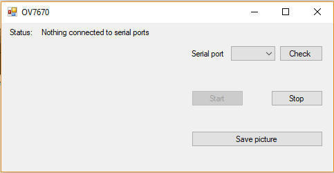
پس از آپلود کد های فوق بر روی آردوینو و اتصال دوربین به آردوینو ، برنامه را که لینک آن در بالا قرار داده شد بود دانلود و آن را اجرا کنید سپس پورتی را که آردوینو به آن متصل است انتخاب کنید تا تصاویر نمایش داده شوند .
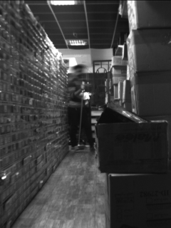
تصویر زیر با ماژول OV7670 گرفته شده است :
سلام.
ببخشید من هر کاری می کنم دوربینم هیچ تصویری رو توی نرم افزار نشون نمیده و صفحه خالیه. میشه راهنماییم کنید؟ ممنون
سلام وقت شما بخیر . اگر در انتخاب پورت COM و باز کردن پورت ، برنامه هیچ خطایی نمی گیرد احتمالا دوربین رو به درستی به آردوینو متصل نکردید . بعضی وقتا به دلیل قطعی در سیم های برد بوردی و خود برد بورد ها این مشکل پیش میاد .
سلام تو مدار میشه توضیح بدین چطوری فرکانس ۴۸mhرو میشه با میکرو تولید کرد
سلام،
علت تار بودن تصویر و اینکه اصلا تصویر واضحی دیده نمیشه را چیه؟؟؟
سلام در کامپایل کردن برنامه در ۴۴۶ ارور داد
سلام ببخشید من لینکی نمی بیسنم
سلام من کد رو کپی کردم توی محیط برنامه نویسی آردوینو ولی این خطا رو نمایش میده
لطفا راهنمایی کنید
سلام
آیا با این دوربین میشه تصویر رنگی هم گرفت؟
سلام ببخشی د من نمیدونم چرا به کد غلط املایی می گیره؟ می شه راهنمایی کنید.ممنونم
سلام خسته نباشید ببخشید من میخوام دوربین بزارم روی هواپیمام میخوام برام در هین پرواز فیلم رو ارسال کنه. این ماژول همچین قابلیتی داره یا باید از یه ماژل دوربین دیگه استفاده کنم؟لطفا بگید
Reset دوربین یه بار ۳v اردوینو uno رو اشغال کرده
در پایان هم اخرین pin هم ۳v رو اشغال میکنه
این شماتیک مشکل داره فکر میکنم